(China (Mainland))

Product Summary
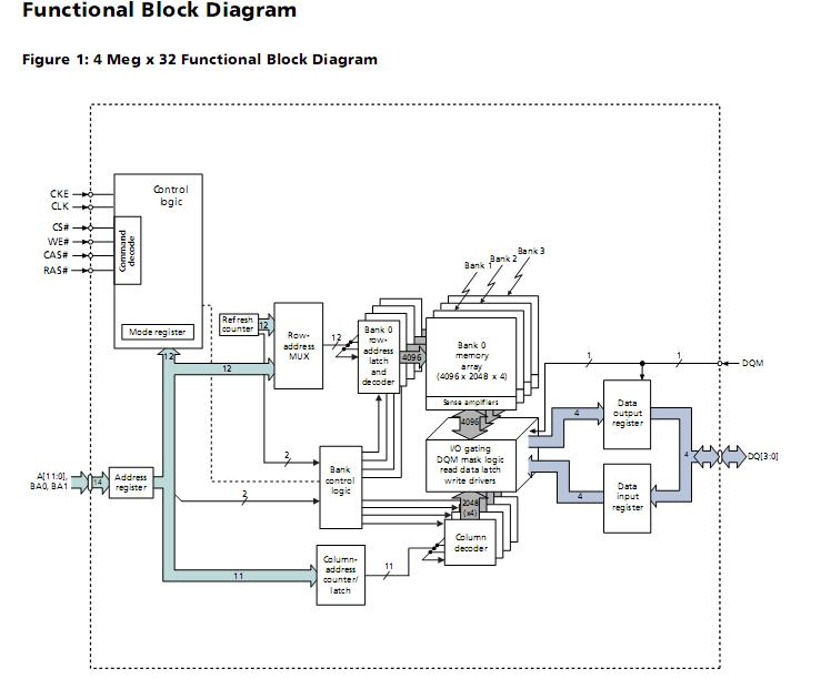
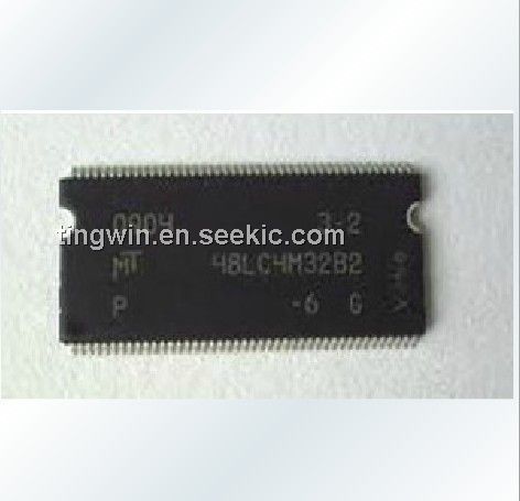
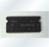
The MT48LC4M32B2P-6G is a high-speed CMOS, dynamic random-access memory containing 134,217,728 bits. The MT48LC4M32B2P-6G is internally configured as a quad-bank DRAM with asynchronous interface (all signals are registered on the positive edge of the clock signal, CLK) . Read and write accesses to the mt48lc4M32b2p-6g are burst oriented; accesses start at a selected location and continue for a programmed number of locations in a programmed sequance. provides for programmable read or write burst lengths (BL) of 1, 2, 4, or 8 locations, or the full page, with a burst terminate option. The MT48LC4M32B2P-6G uses an internal pipelined architecture to achieve high-speed operation.
Parametrics
MT48LC4M32B2P-6G absolute maximum ratings: (1) Voltage on VDD , VDDQ supply relative to VSS, VDD, VDDQ: -1 to 4.6V; (2) Voltage on inputs, NC, or I/O pins relative to VSS, VIN: -1 to 4.6V; (3) Storage temperature (plastic) TSTG: -55 to 150°C; (4) Power dissipation: 1W.
Features
MT48LC4M32B2P-6G features: (1) PC100-compliant; (2) Fully synchronous; all signals registered on positive edge of system clock; (3) Internal pipelined operation; column address can be changed every clock cycle; (4) Internal banks for hiding row access/precharge; (5) Programmable burst lengths: 1, 2, 4, 8, or full page; (6) Auto precharge, includes concurrent auto precharge and auto refresh modes; (7) Self refresh mode (not available on AT devices) ; (8) Auto refresh: 64ms, 4096-cycle refresh (commercial and industrial) , 16ms, 4096-cycle refresh (automotive) ; (9) LVTTL-compatible inputs and outputs; (10) Single 3.3V± 0.3V power supply; (11) Supports CAS latency (CL) of 1, 2, and 3.
Diagrams