(China (Mainland))


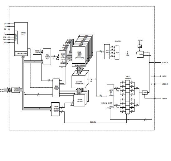
Product Summary
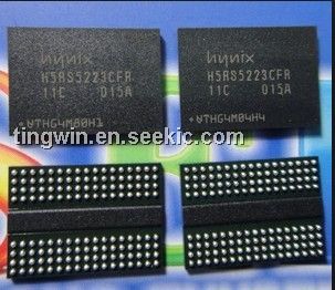
The h5rs5223cfr-11c is a 512Mbit (16Mx32) GDDR3 SDRAM. The h5rs5223cfr-11c is a high-speed CMOS, dynamic random-access memory containing 536,870,912 bits. The h5rs5223cfr-11c is internally configured as a eight-bank DRAM. The h5rs5223cfr-11c uses a double data rate architecture to achieve high-speed opreration. A single read or write access for the h5rs5223cfr-11 cconsists of a 4n-bit wide, every two-clock-cycles data transfer at the internal DRAM core and two corresponding n-bit wide, one-half-clock-cycle data transfers at the I/O pins.
Parametrics
h5rs5223cfr-11c absolute maximum ratings: (1) Voltage on Vdd Supply Relative to Vss: -0.5 to +2.5V; (2) Voltage on VddQ Supply Relative to Vss: -0.5 to +2.5V; (3) Voltage on Vref and Inputs Relative to Vss: -0.5 to +2.5V; (4) Voltage on I/O Pins Relative to Vss: -0.5 to VddQ +0.5V; (5) MAX Junction Temperature, TJ: +125°C; (6) Storage Temperature (plastic) : -55 to +150°C; (7) Power Dissipation: TBD; (8) Short Circuit Output Current: 50mA.
Features
h5rs5223cfr-11c features: (1) 2.05V/ 1.8V/ 1.5V power supply supports; (2) Single ended WRITE Strobe (WDQS) per byte; (3) Internal, pipelined double-data-rate (DDR) architecture; two data accesses per clock cycle; (4) On Die Termination; (5) Output Driver Strength adjustment by EMRS; (6) Calibrated output driver; (7) Commands entered on each positive CK edge; (8) RDQS edge-aligned with data for READ; with WDQS center-aligned with data for WRITE; (9) 8 internal banks for concurrent operation; (10) CAS Latency: 4~11 (clock) ; (11) Data mask (DM) for masking WRITE data; (12)Programmable burst lengths: 4, 8; (13) Auto precharge option; (14) Auto Refresh and Self Refresh Modes; (15) Concurrent Auto Precharge support; (16) tRAS lockout support, Active Termination support; (17) Programmable Write latency(1, 2, 3, 4, 5, 6) ; (18) Boundary Scan Function with SEN pin; (19) Mirror Function with MF pin.
Diagrams